New Materials, New Nanostructures, New Properties
Created by physical vapor deposition
We control atomistic processes during physical vapor deposition in order to create new materials and nanostructures with unique new physical properties. Some projects focus more on understanding the actual process of making new materials including controlling their micro- and nanostructures, while other projects study the properties of new materials or how these properties are affected by the nanoscale structure. For most projects, materials synthesis and characterization is complemented by first-principles simulations. The pictures below illustrate some of the projects. Details can be found in our publications.
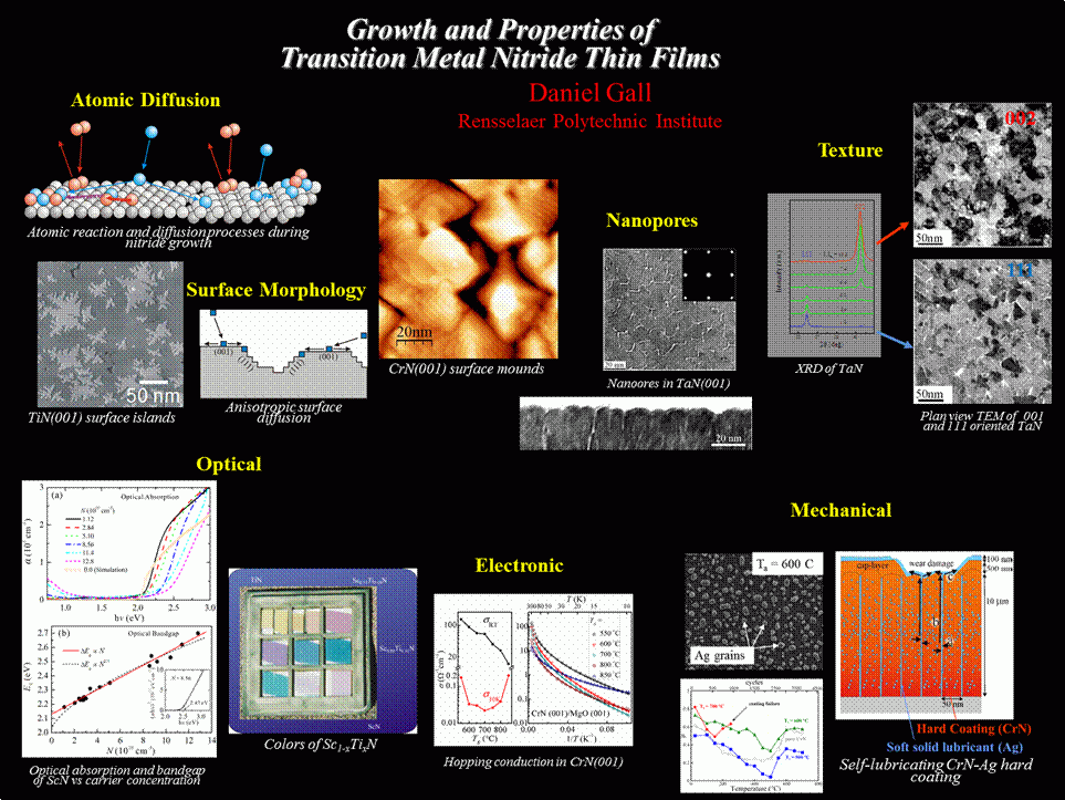
(1) Growth and properties of transition metal nitride thin films
An atomistic understanding of the thin film growth process is developed by combining research on multiple length scales including single atom diffusion and reaction pathways, the formation of surface islands, the development of a surface morphology, the formation of nanopores, and the texture and phase formation in polycrystalline layers. Optical and electron transport properties of new semiconductors (e.g. ScN, CrN) are studied by both measurements and simulations, and new functional hard coating materials developed, including self-lubricating nanoporous CrN with Ag inclusions.
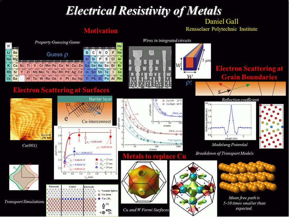
(2) Electrical resistivity of metals
Motivated by the semiconductor industry which is concerned by the increasing resistivity with decreasing Cu wire dimensions, we study electron scattering at surfaces and grain boundaries and develop methods to suppress electron scattering, resulting in highly conductive metal nanowires. The work involves growth of thin single-crystal layers, electron transport measurements, and simulations.
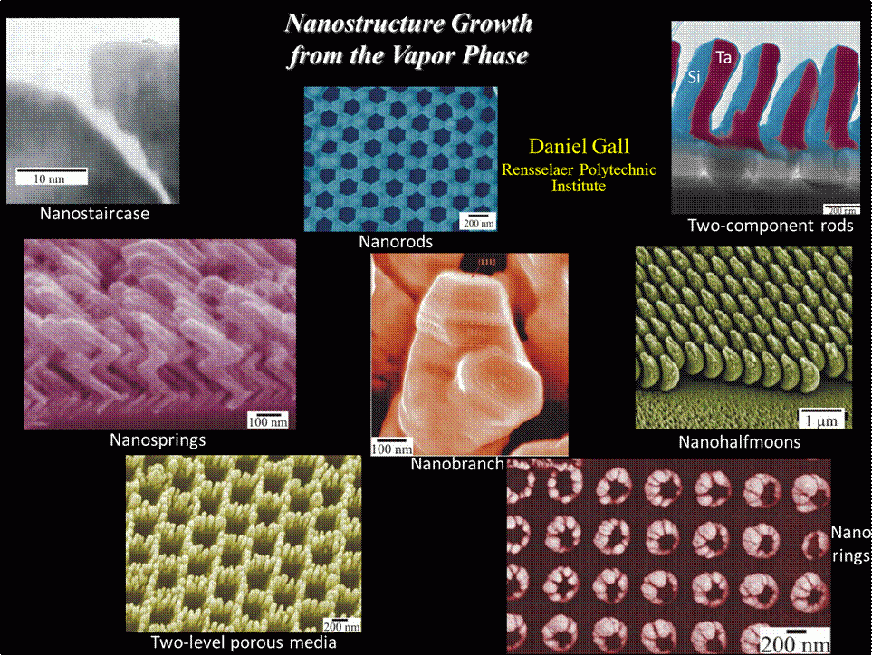
(3) Nanostructure growth from the vapor phase
We exploit atomic shadowing and anisotropic surface diffusion to create various arrays of nanostructures using physical vapor deposition. This work involves patterning by self-assembly, followed by nanostructure growth and microstructural analyses.