Multi-chamber ultra-high vacuum deposition system
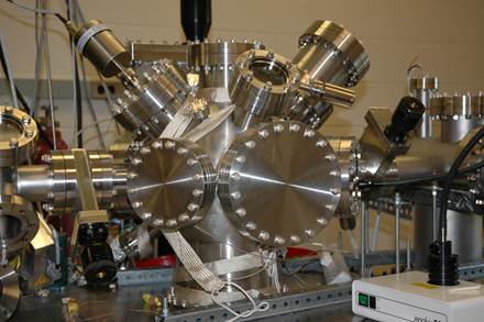
The most important tool in our laboratory is a unique multi-chamber deposition and analysis system used to grow epitaxial transition metal nitride layers, nanostructure arrays by glancing angle deposition, and single crystal metal films. At its core is a magnetron sputter deposition chamber with ports for simultaneous deposition from up to seven sources from various angles. The substrate holder allows continuous azimuthal rotation, heating up to 1200 oC, and rf and dc biasing in order to apply controlled ion-irradiation during growth. Polar angles are adjusted by a linear z-shift. The system also contains an e-beam source for deposition by evaporation and a HIPIMS power supply for ionized deposition.
Newly grown samples can be transferred in vacuum to the adjacent analysis chamber which contains an electronic transport measurement system and an Omicron scanning tunneling microscope.
Supercomputer
Gall's group also employs first principles simulations to study atomic bonding, phase formation, and electron transport, using one of the most powerful university-based supercomputers, a one petaflop 81,920 core IBM BlueGene/Q system operated by the Center for Computational Innovations at Rensselaer Polytechnic Institute.
Materials characterization
Members of Gall's research group use a large set of materials characterization tools available within their own laboratory, the Material Research Center, Core Research Facilities, and the Clean Room at Rensselaer Polytechnic Institute, including:
X-ray diffraction:
- PANalytical XPert PRO Theta/Theta Powder XRD system with an open Eulerian cradle, a PIXcel array detector, an x-ray mirror, a hybrid monochromator, a high-temperature stage (1200 oC), an alternate Ag-source for pair correlation measurements, Diamond anvil cell for high-pressure high-temperature (600 oC) measurements
- Bruker D8 Discover X-Ray Diffractometer with a Centric Eulerian cradle, x-ray mirror, four-bounce incident and three-bounce diffracted beam monochromators, in-plane diffraction, temperature stage (-100 to 350 oC).
Auger Electron and Photoelectron Spectroscopy:
- Physical Electronics PHI 700 Scanning Auger Nanoprobe (field emission source, cylindrical mirror analyzer, 6 nm beam diameter, sputter gun).
- PHI 5000 VersaProbe Scanning ESCA Microprobe (focused 10 mm monochromatic x-ray source, Ar ion gun, 16-channel detector, He-source for UPS) with an attached multi-chamber sample processing system including e-beam evaporation, reaction chamber (30-900 oC, 10-4-105 Pa reactive gas).
Electron Transport:
- in situ linear 4-point-probe integrated in an analysis chamber that is attached to the above sputter deposition system, providing electron transport measurement capabilities without air exposure of the samples.
- Cryo-magnetics Inc. 4He cryostat system with a temperature range from 4-300 K and a 5 T superconducting magnet.
- sputter deposition system to fabricate contacts in a VanderPauw geometry.
- Jandel linear spring loaded 4-point probe for 77-300 K measurements for fast low-temperature measurements without need for patterning or contact deposition.
Optical Spectroscopy:
- Four different FTIR systems, including a Bruker Vertex 70 FTIR Spectroscope with PIKE ATR Accessory (8000-350 cm-1), and a Nicolet Magna IR-560 FTIR (5000-334 cm-1) for both transmission and reflection.
- Three different UV-VIS-IR spectrophotometers, including a Perkin-Elmer Lambda 950 (250-2500 nm) and a Perkin Elmer Lambda 650 UV-Vis with a Diffuse Reflectance module and an integrating sphere.
Scanning electron microscopy:
- Carl Zeiss Ultra 1540 Dual Beam FIB/SEM System (CANION 31 FIB Column, GEMINI Electron Optical Column, 1.1 nm resolution at 20 kV, STEM and EDX detector).
- Carl Zeiss Supra SEM with direct write attachment (1.5 nm resolution at 15 kV), - JEOL JSM-6332 FESEM (Field Emission, 0.5 - 30 kV, 1.5 nm resolution at 15 kV, Equipped with Secondary, Backscattered and Cathode luminescence detectors).
- JEOL JSM-840 SEM (W, 0.2 - 35kV, 5 nm resolution at 35 kV, Equipped with detectors for Secondary and Backscattered electron signals, and an EDS attachment)
Transmission electron microscopy:
- JEM-2010 FASTEM (LaB6, 200 kV, 0.14 nm resolution, Equipped with Oxford EDS, ASID (STEM), FASTEM, Gatan GIF and Gatan EELS for spatially resolved spectroscopy)
- Philips CM 12 TEM (LaB6, 120 kV, 0.24 nm resolution, Equipped with EDS and small CCD attachment).
Nanoindentation, Tribology, and Atomic Force Microscopy:
- Hysitron Nanotribometer capable of nano indentation and nanoDMA using an integrated AFM for indent-surface analysis.
- Nanovea Series ball-on-disk tribometer with vacuum or controlled atmosphere and heating up to 800 oC and a Nanovea ST400 non-contact optical profilometer for friction and wear tests
- Dimension 3100 Digital Instruments (DI) AFM with a Nanoscope IIIe controller and an Extender Electronics Module allows scanning surface potential microscopy (SSPM).
- Multimode DI AFM with a Nanoscope IV controller and a high temperature heater is designed for high resolution imaging at various temperatures and inert gas environments.
Patterning, electrical characterization:
A class-100 clean room in the Center for Integrated Electronics at Rensselaer houses an extensive range of equipment, including thin film deposition (CVD, evaporation, sputtering), photolithography, reactive ion etching, e-beam lithography, focused ion beam patterning, ellipsometry, resistivity, and many other tools.
Brillouin and Raman Scattering:
- six-pass high contrast Fabry-Perot interferometer (JSR Scientific Instruments) for measuring the elastic moduli of materials
- HR800 micro-Raman system (Horiba Jobin Yvon) equipped with a confocal microscope attachment and a charge-coupled detector (CCD), using a 532 nm (Coherent Verdi-V2 diode-pumped solid-state (DPSS), single-frequency, continuous wave) laser and a 1500 oC in-situ heating stage with environmental control.
High-pressure characterization:
- membrane-driven diamond anvil cell (DAC) with pressures up to 30 GPa for in situ Raman and Brillouin measurements,
- membrane-driven DAC (20 GPa) with heating up to 600 oC for in situ x-ray diffraction measurements with a Ag x-ray point source and a PanAnalytical diffractometer.